Semiconductors have transformed the world we live in, powering our devices and enabling technological advancements.
These materials, often composed of silicon or other semiconducting compounds, possess unique properties that allow for the control and manipulation of electrical current.
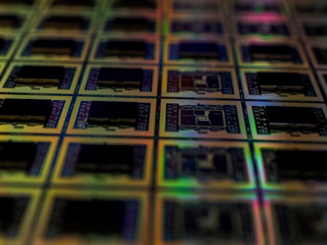
However, within the realm of semiconductors lies a hidden world of imperfections known as microstructural defects.
Microstructural defects, as the name suggests, are tiny irregularities in the arrangement of atoms and crystal structures within semiconductors.
These defects can arise during the semiconductor manufacturing process and have the potential to impact their performance and reliability.
Understanding these defects is crucial for optimizing semiconductor technology and ensuring high-quality production.
One powerful technique that has emerged as a valuable tool in the analysis of microstructural defects is Electron Beam Induced Current (EBIC).
EBIC allows researchers to investigate the electrical behavior of semiconductors at high resolution, providing valuable insights into the nature and impact of these defects.
Unraveling the Intricate World of Microstructural Defects Through EBIC Imaging
EBIC imaging allows scientists to visualize and study the electrical activity within semiconductors, making it an invaluable tool for the analysis of microstructural defects.
By utilizing a finely focused electron beam, researchers can generate localized electron-hole pairs within the semiconductor material.
These pairs exhibit different currents depending on the presence or absence of defects, which can be detected by the EBIC technique.
Through this imaging technique, researchers can directly observe and identify various types of defects, such as dislocations, stacking faults, and point defects.
Dislocations, for example, are disruptions in the periodic arrangement of atoms, resulting in regions of strain within the crystal lattice.
EBIC imaging enables the precise characterization of these defects, providing a deeper understanding of their influence on material properties and device performance.
By mapping the electrical behavior of defects, scientists can gain insights into their effects on charge transport, carrier concentration, and recombination processes.
This information is crucial for optimizing semiconductor fabrication processes and developing strategies to mitigate the impact of defects, ultimately leading to enhanced device performance and reliability.
Understanding the Impact of Defects on Semiconductor Performance and Reliability
The presence of microstructural defects in semiconductors can have profound implications on their electrical and optical properties.
Even minor defects can significantly affect the efficiency and reliability of electronic devices.
Understanding these effects is vital for improving device performance and developing new technologies.
Defects can introduce additional energy levels within the semiconductor bandgap, leading to trap states that impede charge carrier movement.
This can result in reduced carrier mobility, increased recombination rates, and altered electrical conductivity.
Consequently, devices fabricated from defective semiconductors may experience reduced efficiency and slower operation speeds.
Furthermore, defects can influence optical properties by modifying the absorption and emission characteristics of semiconductors.
For instance, point defects such as vacancies or interstitials can introduce localized energy states that impact the band structure and alter the semiconductor’s photoluminescence spectrum.
EBIC, with its ability to correlate microstructural defects with electrical behavior, plays a crucial role in identifying and characterizing these phenomena.
By understanding the impact of defects on semiconductor performance, researchers can devise strategies to mitigate their effects and improve the reliability and efficiency of electronic devices.
Examining Different Viewpoints on the Significance of Microstructural Defects in Semiconductor Manufacturing
The significance of microstructural defects in semiconductor manufacturing is a topic of much debate within the industry.
Some argue that defects are inherently detrimental and must be eliminated to ensure high-quality production, while others believe that defects can sometimes have beneficial effects or serve as an avenue for innovation.
On one hand, defects can introduce undesirable variations in device characteristics, compromising yield and overall reliability.
In high-performance applications like microprocessors, even a single defect can lead to catastrophic failures that render devices unusable.
In such cases, meticulous defect detection and mitigation strategies are implemented to ensure the highest possible quality standards.
On the other hand, certain defects can be intentionally induced or engineered to tailor the properties of semiconductors for specific applications.
These controlled defects, known as intentional doping or dopant atoms, are introduced precisely to modify the semiconductor’s electrical behavior, enabling the creation of different functionalities.
For instance, in photovoltaic devices, dopants can be strategically placed to facilitate charge separation and enhance energy conversion efficiency.
While intentional defects are carefully designed, unintentional defects can still arise during the manufacturing process.
The challenge lies in distinguishing between intentional and unintentional defects, understanding their impact, and developing effective strategies to harness their beneficial effects while minimizing adverse consequences.
EBIC provides a powerful tool for identifying and differentiating between these defect types, enabling researchers to make informed decisions about their significance in semiconductor manufacturing.
The Leading Brand Advantage
When it comes to unlocking the secrets of microstructural defects in semiconductors, Wintech Nano is at the forefront of cutting-edge research and innovation.
With a focus on developing advanced analytical techniques and high-resolution imaging tools, this tech company empowers scientists and engineers to push the boundaries of semiconductor analysis.
By leveraging the power of EBIC and other groundbreaking technologies, the company helps researchers gain unparalleled insights into the world of microstructural defects.
By enabling precise defect characterization, their solutions play a pivotal role in optimizing device performance, improving yield, and driving technological advancements.
Personal Perspectives: Embracing Imperfections as Pathways to Innovation
In the quest for perfection and semiconductor quality, it is easy to overlook the potential benefits that defects can offer.
Personally, I find it fascinating how imperfections can sometimes serve as pathways to innovation and unforeseen discoveries.
Historically, numerous breakthroughs have arisen from the exploration of semiconductor defects.
One notable example is the creation of the point-contact transistor, pioneered by William Shockley in 1947.
This groundbreaking invention, which relied on the controlled fabrication of a defective region within the semiconductor material, paved the way for modern electronic devices and revolutionized the field of electronics.
Acknowledging the potential of imperfections to inspire innovation allows us to embrace a more holistic approach to semiconductor manufacturing.
By leveraging advanced analytical techniques like EBIC, we can strike a balance between defect detection and intentional defect manipulation, effectively harnessing the power of imperfections to drive technological progress.
Conclusion
Microstructural defects are a fascinating aspect of semiconductor technology that can significantly impact device performance and reliability.
Unlocking the secrets behind these defects is essential for optimizing semiconductor manufacturing and driving innovation in electronic devices.
With the emergence of powerful analytical techniques like Electron Beam Induced Current (EBIC), researchers can delve into the intricate world of microstructural defects, gaining unprecedented insights into their nature, behavior, and significance.
Armed with this knowledge, scientists can develop strategies to minimize the adverse effects of defects while capitalizing on their potential benefits.
Wintech Nano, with its commitment to cutting-edge research and innovative solutions, revolutionizes the analysis of microstructural defects in semiconductors.
By leveraging EBIC and other advanced technologies, this tech laboratory empowers the semiconductor industry to unlock the full potential of these fascinating imperfections.